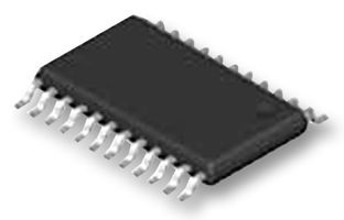
PLL Clock Driver, 1-to-9 output configuration, operating at up to 125MHz. Features LVTTL input and gold contact plating. Housed in a 24-TSSOP surface mount package, this component operates within a 3V to 3.6V supply voltage range. RoHS compliant and lead-free, with a maximum operating temperature of 70°C.
Frequency125MHz
PackageTSSOP
Current10uA
MountingSurface Mount
Quick Jump:
Technical Specifications
Texas Instruments CDC2509BPWG4 technical specifications.
General
| Package/Case | TSSOP |
| Contact Plating | Gold |
| Frequency | 125MHz |
| Input | LVTTL |
| Lead Free | Lead Free |
| Max Frequency | 125MHz |
| Max Operating Temperature | 70°C |
| Min Operating Temperature | 0°C |
| Max Supply Voltage | 3.6V |
| Min Supply Voltage | 3V |
| Mount | Surface Mount |
| Number of Circuits | 1 |
| Number of Elements | 1 |
| Number of Outputs | 9 |
| Operating Supply Voltage | 3.3V |
| Package Quantity | 60 |
| Packaging | Rail/Tube |
| PLL | Yes |
| Power Dissipation | 700mW |
| Quiescent Current | 10uA |
| Radiation Hardening | No |
| RoHS Compliant | Yes |
| Series | CDC2509B |
| Supply Current | 10uA |
| Weight | 0.003157oz |
Compliance
| RoHS | Compliant |
Datasheet
Texas Instruments CDC2509BPWG4 Datasheet
Download the complete datasheet for Texas Instruments CDC2509BPWG4 to view detailed technical specifications.
This datasheet cannot be embedded due to technical restrictions.
Product Images

