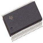
The CDC2516DGGRG4 is a clock buffer IC with a maximum operating frequency of 125MHz and an operating supply voltage of 3.3V. It is designed for use with LVTTL input signals and is packaged in a lead-free TSSOP-48 package. The device is RoHS compliant and has a maximum supply voltage of 3.6V. It operates within a temperature range of 0°C to 70°C and has a supply current of 20uA. The CDC2516DGGRG4 is a single circuit device with 16 outputs.
Checking distributor stock and pricing after the page loads.
Sign in to ask questions about the Texas Instruments CDC2516DGGRG4 datasheet using AI. Get instant answers about specifications, features, and technical details, ideal for finding information in larger documents.
Sign In to ChatWidest selection of semiconductors and electronic components in stock and ready to ship ™
| Package/Case | TSSOP |
| Contact Plating | Gold |
| Frequency | 125MHz |
| Input | LVTTL |
| Lead Free | Lead Free |
| Max Frequency | 125MHz |
| Max Operating Temperature | 70°C |
| Min Operating Temperature | 0°C |
| Max Supply Voltage | 3.6V |
| Min Supply Voltage | 3V |
| Mount | Surface Mount |
| Number of Circuits | 1 |
| Number of Elements | 1 |
| Number of Outputs | 16 |
| Operating Supply Voltage | 3.3V |
| Package Quantity | 2000 |
| Packaging | Tape and Reel |
| PLL | Yes |
| Radiation Hardening | No |
| RoHS Compliant | Yes |
| Series | CDC2516 |
| Supply Current | 20uA |
| Weight | 0.007873oz |
| RoHS | Compliant |
Download the complete datasheet for Texas Instruments CDC2516DGGRG4 to view detailed technical specifications.
The embedded preview will load automatically when this section scrolls into view.