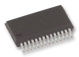
10-output clock fanout buffer, surface mount, SSOP package with gold contact plating. Operates at a maximum frequency of 100MHz, with a nominal supply current of 200µA. Features LVTTL input and a 3.3V operating supply voltage range of 3.135V to 3.465V. RoHS compliant and lead-free, suitable for operation between 0°C and 70°C.
Sign in to ask questions about the Texas Instruments CDC319DBG4 datasheet using AI. Get instant answers about specifications, features, and technical details, ideal for finding information in larger documents.
Sign In to ChatWidest selection of semiconductors and electronic components in stock and ready to ship ™
Texas Instruments CDC319DBG4 technical specifications.
| Package/Case | SSOP |
| Contact Plating | Gold |
| Frequency | 140MHz |
| Input | LVTTL |
| Lead Free | Lead Free |
| Max Frequency | 100MHz |
| Max Operating Temperature | 70°C |
| Min Operating Temperature | 0°C |
| Max Supply Voltage | 3.465V |
| Min Supply Voltage | 3.135V |
| Mount | Surface Mount |
| Nominal Supply Current | 200uA |
| Number of Circuits | 1 |
| Number of Outputs | 10 |
| Operating Supply Voltage | 3.3V |
| Package Quantity | 50 |
| Packaging | Rail/Tube |
| Propagation Delay | 2000ns |
| Quiescent Current | 500uA |
| Radiation Hardening | No |
| RoHS Compliant | Yes |
| Series | CDC319 |
| Turn-On Delay Time | 2000ns |
| Weight | 0.007351oz |
| RoHS | Compliant |
Download the complete datasheet for Texas Instruments CDC319DBG4 to view detailed technical specifications.
The embedded preview will load automatically when this section scrolls into view.