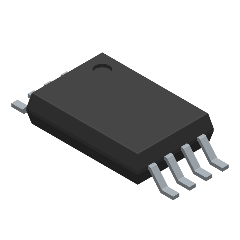
2-output, 1-input clock fanout buffer operating up to 250MHz. Features LVCMOS input and gold contact plating. Surface mountable in a 8-pin TSSOP package with dimensions of 4.5mm length, 3.1mm width, and 1.05mm height. Operates from a 2.3V to 3.6V supply voltage with a maximum supply current of 10mA. RoHS compliant with a propagation delay of 2.6ns.
Checking distributor stock and pricing after the page loads.
Sign in to ask questions about the Texas Instruments CDCLVC1102PW datasheet using AI. Get instant answers about specifications, features, and technical details, ideal for finding information in larger documents.
Sign In to ChatWidest selection of semiconductors and electronic components in stock and ready to ship ™
| Package/Case | TSSOP |
| Contact Plating | Gold |
| Frequency | 250MHz |
| Height | 1.05mm |
| Input | LVCMOS |
| Lead Free | Lead Free |
| Length | 4.5mm |
| Max Frequency | 250MHz |
| Max Operating Temperature | 85°C |
| Min Operating Temperature | -40°C |
| Max Supply Current | 10mA |
| Max Supply Voltage | 3.6V |
| Min Supply Voltage | 2.3V |
| Mount | Surface Mount |
| Number of Circuits | 1 |
| Number of Outputs | 2 |
| Package Quantity | 150 |
| Packaging | Rail/Tube |
| Propagation Delay | 2.6ns |
| Radiation Hardening | No |
| Reach SVHC Compliant | No |
| RoHS Compliant | Yes |
| Supply Current | 6mA |
| Turn-On Delay Time | 10ns |
| Width | 3.1mm |
| RoHS | Compliant |
Download the complete datasheet for Texas Instruments CDCLVC1102PW to view detailed technical specifications.
The embedded preview will load automatically when this section scrolls into view.
