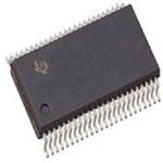
2.5V Phase Lock Loop (PLL) DDR Clock Driver, operating at up to 220MHz. This surface mount integrated circuit features 10 outputs and SSTL-2 input compatibility. Housed in a 48-TSSOP package with gold contact plating, it offers a wide operating temperature range of -40°C to 85°C. RoHS compliant and lead-free, this clock buffer and driver is designed for efficient signal distribution.
Checking distributor stock and pricing after the page loads.
Sign in to ask questions about the Texas Instruments CDCVF857DGGG4 datasheet using AI. Get instant answers about specifications, features, and technical details, ideal for finding information in larger documents.
Sign In to ChatWidest selection of semiconductors and electronic components in stock and ready to ship ™
| Package/Case | TSSOP |
| Contact Plating | Gold |
| Frequency | 220MHz |
| Height | 1.15mm |
| Input | SSTL-2 |
| Lead Free | Lead Free |
| Length | 12.5mm |
| Max Frequency | 220MHz |
| Max Operating Temperature | 85°C |
| Min Operating Temperature | -40°C |
| Max Supply Current | 10mA |
| Max Supply Voltage | 2.7V |
| Min Supply Voltage | 2.18V |
| Mount | Surface Mount |
| Number of Circuits | 1 |
| Number of Elements | 1 |
| Number of Outputs | 10 |
| Operating Supply Voltage | 2.5V |
| Package Quantity | 40 |
| Packaging | Rail/Tube |
| PLL | Yes |
| Radiation Hardening | No |
| RoHS Compliant | Yes |
| Series | CDCVF857 |
| Supply Current | 10mA |
| Weight | 0.007873oz |
| Width | 6.1mm |
| RoHS | Compliant |
Download the complete datasheet for Texas Instruments CDCVF857DGGG4 to view detailed technical specifications.
The embedded preview will load automatically when this section scrolls into view.