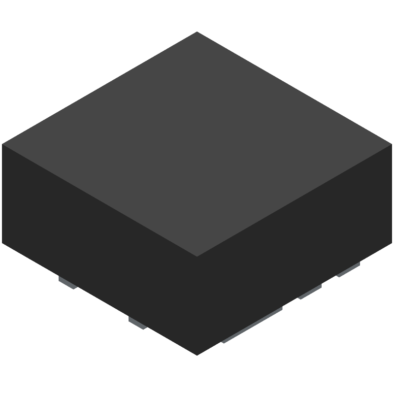
Synchronous buck power stage featuring an 8-pin SON EP package. This integrated circuit operates across a wide temperature range from -55°C to 150°C, suitable for military applications. It includes a buffer or inverter-based MOSFET driver interface, designed for a nominal supply voltage of 12V with a maximum of 22V. The component has a dual terminal position and a JEDEC package code of S-PDSO-N8, with dimensions of 3.3mm x 3.3mm.
Sign in to ask questions about the Texas Instruments CSD86330Q3D datasheet using AI. Get instant answers about specifications, features, and technical details, ideal for finding information in larger documents.
Sign In to ChatWidest selection of semiconductors and electronic components in stock and ready to ship ™
Texas Instruments CSD86330Q3D technical specifications.
| Max Operating Temperature | 150 |
| Number of Terminals | 8 |
| Min Operating Temperature | -55 |
| Terminal Position | DUAL |
| JEDEC Package Code | S-PDSO-N8 |
| Width | 3.3 |
| Length | 3.3 |
| Pin Count | 8 |
| Number of Functions | 1 |
| Temperature Grade | MILITARY |
| Supply Voltage-Nom | 12 |
| Supply Voltage-Max | 22 |
| Interface IC Type | BUFFER OR INVERTER BASED MOSFET DRIVER |
| Input Characteristics | STANDARD |
| RoHS | No |
| Eccn Code | EAR99 |
| Lead Free | Yes |
| HTS Code | 8541.29.00.95 |
| REACH | not_compliant |
| Military Spec | False |
Download the complete datasheet for Texas Instruments CSD86330Q3D to view detailed technical specifications.
The embedded preview will load automatically when this section scrolls into view.