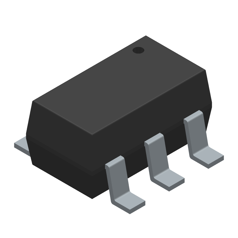
The SN6505BQDBVRQ1 is a 5V interface circuit from Texas Instruments, designed for automotive applications. It operates within a temperature range of -40°C to 125°C and is packaged in a 6-pin LSSOP. The device has a nominal supply voltage of 5V, with a minimum and maximum voltage range of 2.25V and 5.5V, respectively. It meets the AEC-Q100 screening level and is suitable for use in various interface applications.
Checking distributor stock and pricing after the page loads.
Sign in to ask questions about the Texas Instruments SN6505BQDBVRQ1 datasheet using AI. Get instant answers about specifications, features, and technical details, ideal for finding information in larger documents.
Sign In to ChatWidest selection of semiconductors and electronic components in stock and ready to ship ™
| Max Operating Temperature | 125 |
| Number of Terminals | 6 |
| Min Operating Temperature | -40 |
| Terminal Position | DUAL |
| JEDEC Package Code | R-PDSO-G6 |
| Width | 1.6 |
| Length | 2.9 |
| Number of Functions | 1 |
| Temperature Grade | AUTOMOTIVE |
| Supply Voltage-Nom | 5 |
| Supply Voltage-Min | 2.25 |
| Supply Voltage-Max | 5.5 |
| Screening Level | AEC-Q100 |
| Interface IC Type | INTERFACE CIRCUIT |
| RoHS | Yes |
| Lead Free | Yes |
| REACH | Compliant |
| Military Spec | False |
Download the complete datasheet for Texas Instruments SN6505BQDBVRQ1 to view detailed technical specifications.
The embedded preview will load automatically when this section scrolls into view.