
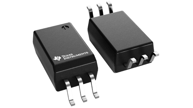
This single-channel isolated gate driver is intended for IGBTs, MOSFETs, and SiC MOSFETs and uses an opto-compatible emulated-diode input stage. It provides 4.5-A source and 5.3-A sink peak output current, supports up to 33 V output supply voltage, and offers 3.75-kVRMS basic isolation. The device specifies up to 105 ns propagation delay, 25 ns maximum part-to-part delay matching, 35 ns maximum pulse-width distortion, and at least 150 kV/µs common-mode transient immunity. It is offered in a stretched SO-6 package with more than 8.5 mm creepage and clearance, CTI greater than 600 V, and an operating junction temperature range of -40°C to 150°C.
Checking distributor stock and pricing after the page loads.

Sign in to ask questions about the Texas Instruments UCC23313DWYR datasheet using AI. Get instant answers about specifications, features, and technical details, ideal for finding information in larger documents.
Sign In to ChatWidest selection of semiconductors and electronic components in stock and ready to ship ™
| Max Operating Temperature | 125 |
| Number of Terminals | 6 |
| Min Operating Temperature | -40 |
| Terminal Position | DUAL |
| JEDEC Package Code | R-PDSO-G6 |
| Number of Functions | 1 |
| Temperature Grade | AUTOMOTIVE |
| Interface IC Type | BUFFER OR INVERTER BASED IGBT/MOSFET DRIVER |
| RoHS | Yes |
| Lead Free | Yes |
| REACH | Compliant |
| Military Spec | False |
Download the complete datasheet for Texas Instruments UCC23313DWYR to view detailed technical specifications.
The embedded preview will load automatically when this section scrolls into view.
