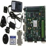
The XC5VLX50FFG676 Evaluation Kit is a development board for the Xilinx XC5VLX50FFG676 FPGA. It features 257MB of RAM and 32MB of linear flash memory. The kit includes USB 2.0, RS232, and SPI interfaces, as well as a DVI/VGA display interface for connecting to CRT or LCD displays. The board also supports JTAG debugging and has 8 LEDs and 13 push buttons and switches for user input.
Checking distributor stock and pricing after the page loads.
Sign in to ask questions about the Xilinx HW-V5-ML501-UNI-G datasheet using AI. Get instant answers about specifications, features, and technical details, ideal for finding information in larger documents.
Sign In to ChatWidest selection of semiconductors and electronic components in stock and ready to ship ™
Xilinx HW-V5-ML501-UNI-G technical specifications.
| Type | Evaluation Kit |
| Supported Device | XC5VLX50FFG676 |
| Supported Device Technology | FPGA |
| RAM Size | 257MB |
| Program Memory Size | 32MB |
| Program Memory Type | Linear Flash/Platform Flash/SPI Flash |
| Main Program Memory Type | Flash |
| USB | 2 |
| RS232 | 1 |
| SPI | 1 |
| Display Interface | DVI/VGA |
| Display Type | CRT/LCD |
| JTAG Support | Yes |
| Number of LEDs | 8 |
| Audio Interfaces | Yes |
| Push Buttons and Switches | 13 |
| Cage Code | 68994 |
| EU RoHS | Yes |
| HTS Code | 9030820000 |
| Schedule B | 9030820000 |
| ECCN | EAR99 |
| Automotive | No |
| AEC Qualified | No |
| PPAP | No |
| Radiation Hardening | No |
| RoHS Versions | 2002/95/EC |
Download the complete datasheet for Xilinx HW-V5-ML501-UNI-G to view detailed technical specifications.
The embedded preview will load automatically when this section scrolls into view.