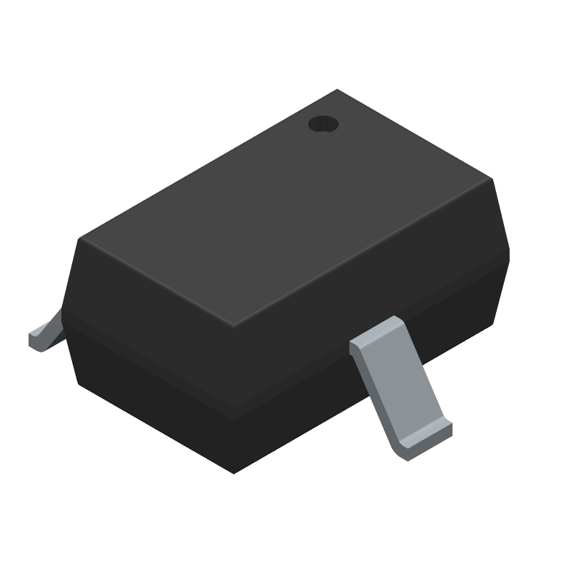
P-Channel JFET, designed for small signal applications. Features a continuous drain current of 630mA and a drain-to-source breakdown voltage of -20V. Operates within a temperature range of -55°C to 150°C with a maximum power dissipation of 300mW. Surface mountable in a SOT-323 package, this silicon MOSFET offers a low on-state resistance of 550mR and fast switching times with turn-on delay of 2.6ns and turn-off delay of 6ns. Halogen and lead-free, it is supplied on tape and reel.
Checking distributor stock and pricing after the page loads.
Sign in to ask questions about the Infineon BSS209PWH6327XTSA1 datasheet using AI. Get instant answers about specifications, features, and technical details, ideal for finding information in larger documents.
Sign In to ChatWidest selection of semiconductors and electronic components in stock and ready to ship ™
| Package/Case | SOT-323 |
| Continuous Drain Current (ID) | 630mA |
| Current Rating | -580mA |
| Drain to Source Breakdown Voltage | -20V |
| Drain to Source Voltage (Vdss) | -20V |
| Gate to Source Voltage (Vgs) | 12V |
| Halogen Free | Halogen Free |
| Height | 0.8mm |
| Input Capacitance | 115pF |
| Lead Free | Lead Free |
| Length | 2mm |
| Max Dual Supply Voltage | -20V |
| Max Operating Temperature | 150°C |
| Min Operating Temperature | -55°C |
| Max Power Dissipation | 300mW |
| Mount | Surface Mount |
| Number of Channels | 1 |
| Number of Elements | 1 |
| On-State Resistance | 550mR |
| Package Quantity | 3000 |
| Packaging | Tape and Reel |
| Power Dissipation | 300mW |
| Radiation Hardening | No |
| Rds On Max | 550mR |
| RoHS Compliant | Yes |
| Series | OptiMOS™ |
| Turn-Off Delay Time | 6ns |
| Turn-On Delay Time | 2.6ns |
| DC Rated Voltage | -20V |
| Width | 1.25mm |
| RoHS | Compliant |
Download the complete datasheet for Infineon BSS209PWH6327XTSA1 to view detailed technical specifications.
The embedded preview will load automatically when this section scrolls into view.
