
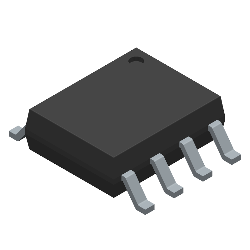
This device is a dual low-side gate driver for power MOSFET and IGBT applications. It operates from a 6 V to 20 V gate-drive supply and provides two independent outputs with typical source and sink peak currents of 2.3 A and 3.3 A. CMOS Schmitt-triggered inputs support 3.3 V and 5 V logic compatibility, and the two channels have matched propagation delays. Typical turn-on and turn-off propagation delays are 50 ns, with typical rise and fall times of 25 ns. The part is specified for ambient operation from -40 °C to 125 °C and is supplied in an SOIC-8N tape-and-reel package.
Checking distributor stock and pricing after the page loads.

Sign in to ask questions about the Infineon IRS4426STRPBF datasheet using AI. Get instant answers about specifications, features, and technical details, ideal for finding information in larger documents.
Sign In to ChatWidest selection of semiconductors and electronic components in stock and ready to ship ™
| Max Operating Temperature | 125 |
| Number of Terminals | 8 |
| Min Operating Temperature | -40 |
| Terminal Position | DUAL |
| JEDEC Package Code | R-PDSO-G8 |
| Width | 3.9 |
| Length | 4.9 |
| Number of Functions | 2 |
| Temperature Grade | AUTOMOTIVE |
| Supply Voltage-Nom | 15 |
| Supply Voltage-Min | 6 |
| Supply Voltage-Max | 20 |
| Interface IC Type | HALF BRIDGE BASED PERIPHERAL DRIVER |
| RoHS | Yes |
| Eccn Code | EAR99 |
| HTS Code | 8542.39.00.01 |
| REACH | Compliant |
| Military Spec | False |
Download the complete datasheet for Infineon IRS4426STRPBF to view detailed technical specifications.
The embedded preview will load automatically when this section scrolls into view.
