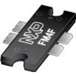
RF MOSFET transistor, N-channel, enhancement mode, single dual drain dual gate configuration. Features 68V maximum drain-source voltage, operating between 1800MHz and 2000MHz. Delivers 60W typical output power with 15.5dB typical power gain, suitable for GSM and GSM EDGE modes. Housed in a 5-pin TO-272 W lead-frame SMT package with flat leads, measuring 23.67mm(Max) length, 9.07mm(Max) width, and 2.64mm(Max) height. Operates across a temperature range of -65°C to 200°C.
PackageTO-272 W
MountingScrew
Power60(Typ)W
Quick Jump:
Technical Specifications
NXP MRF6S18060NB technical specifications.
General
| Basic Package Type | Lead-Frame SMT |
| Package Family Name | TO-272 W |
| Package/Case | TO-272 W |
| Lead Shape | Flat |
| Pin Count | 5 |
| PCB | 5 |
| Package Length (mm) | 23.67(Max) |
| Package Width (mm) | 9.07(Max) |
| Package Height (mm) | 2.64(Max) |
| Seated Plane Height (mm) | 2.64(Max) |
| Pin Pitch (mm) | 5.38 |
| Package Material | Plastic |
| Mounting | Screw |
| Channel Type | N |
| Configuration | Single Dual Drain Dual Gate |
| Channel Mode | Enhancement |
| Number of Elements per Chip | 1 |
| Maximum Drain Source Voltage | 68V |
| Minimum Frequency | 1800MHz |
| Maximum Frequency | 2000MHz |
| Maximum Power Dissipation | 216000mW |
| Min Operating Temperature | -65°C |
| Max Operating Temperature | 200°C |
| Mode of Operation | GSM|GSM EDGE |
| Typical Power Gain | 15.5dB |
| Output Power | 60(Typ)W |
Compliance
| Cage Code | H1R01 |
| EU RoHS | Yes with Exemption |
| HTS Code | 8541290075 |
| Schedule B | 8541290080 |
| ECCN | EAR99 |
| Automotive | No |
| AEC Qualified | No |
| PPAP | No |
| Radiation Hardening | No |
| RoHS Versions | 2011/65/EU, 2015/863 |
Datasheet
NXP MRF6S18060NB Datasheet
Download the complete datasheet for NXP MRF6S18060NB to view detailed technical specifications.
This datasheet cannot be embedded due to technical restrictions.
