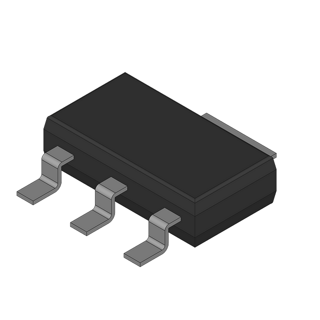
N-channel power MOSFET in SOT package, featuring 55V drain-source breakdown voltage and 150mΩ maximum drain-source on-resistance. This component offers a continuous drain current of 5.5A and a maximum power dissipation of 8.3W. Operating across a temperature range of -55°C to 150°C, it exhibits typical switching times with a turn-on delay of 4.9ns and a fall time of 4.5ns. Packaged on tape and reel, this lead-free MOSFET is designed for efficient power switching applications.
Sign in to ask questions about the NXP PHT6N06T135 datasheet using AI. Get instant answers about specifications, features, and technical details, ideal for finding information in larger documents.
Sign In to ChatWidest selection of semiconductors and electronic components in stock and ready to ship ™
NXP PHT6N06T135 technical specifications.
| Package/Case | SOT |
| Continuous Drain Current (ID) | 5.5A |
| Drain to Source Breakdown Voltage | 55V |
| Drain to Source Resistance | 150mR |
| Drain to Source Voltage (Vdss) | 55V |
| Drain-source On Resistance-Max | 150MR |
| Fall Time | 4.5ns |
| Gate to Source Voltage (Vgs) | 20V |
| Input Capacitance | 175pF |
| Lead Free | Lead Free |
| Max Dual Supply Voltage | 55V |
| Max Operating Temperature | 150°C |
| Min Operating Temperature | -55°C |
| Max Power Dissipation | 8.3W |
| Number of Elements | 1 |
| Package Quantity | 1 |
| Packaging | Tape and Reel |
| Polarity | N-CHANNEL |
| Power Dissipation | 8.3W |
| Radiation Hardening | No |
| Rds On Max | 150mR |
| Series | TrenchMOS™ |
| Turn-Off Delay Time | 7.8ns |
| Turn-On Delay Time | 4.9ns |
| RoHS | Compliant |
Download the complete datasheet for NXP PHT6N06T135 to view detailed technical specifications.
The embedded preview will load automatically when this section scrolls into view.
