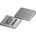
32-bit ARM Cortex M4 RISC microcontroller featuring a 100 MHz maximum clock rate and 256KB Flash program memory. This surface-mount device offers 132KB of RAM, 14 timers, and multiple interfaces including CAN (2), I2C (2), SPI (3), UART (6), I2S (1), and USB (1). Packaged in a 144-pin MAP-BGA with a 1mm pitch, it operates from 1.8V to 3.3V and supports dual ADCs and dual DACs. Extended operating temperature range from -40°C to 105°C.
PackageMAP-BGA
MountingSurface Mount
Quick Jump:
Technical Specifications
NXP PK40DX256VMD10 technical specifications.
General
| Basic Package Type | Ball Grid Array |
| Package Family Name | BGA |
| Package/Case | MAP-BGA |
| Package Description | Molded Array Process Ball Grid Array |
| Lead Shape | Ball |
| Pin Count | 144 |
| PCB | 144 |
| Package Length (mm) | 13 |
| Package Width (mm) | 13 |
| Package Height (mm) | 1.27(Max) |
| Seated Plane Height (mm) | 1.7(Max) |
| Pin Pitch (mm) | 1 |
| Package Material | Plastic |
| Mounting | Surface Mount |
| Family Name | K40 |
| Data Bus Width | 32bit |
| Instruction Set Architecture | RISC |
| Maximum Clock Rate | 100MHz |
| Maximum CPU Frequency | 100MHz |
| Device Core | ARM Cortex M4 |
| Program Memory Type | Flash |
| Program Memory Size | 256KB |
| RAM Size | 132KB |
| Core Architecture | ARM |
| Programmability | Yes |
| Number of Timers | 14 |
| Interface Type | CAN/I2C/I2S/SPI/UART/USB |
| CAN | 2 |
| I2C | 2 |
| SPI | 3 |
| Ethernet | 0 |
| UART | 6 |
| USART | 0 |
| USB | 1 |
| I2S | 1 |
| Max Operating Supply Voltage | 3.6V |
| Min Operating Temperature | -40°C |
| Max Operating Temperature | 105°C |
| Number of ADCs | Dual |
| Number of DACs | Dual |
Compliance
| Cage Code | H1R01 |
| EU RoHS | Yes |
| HTS Code | 8542310001 |
| Schedule B | 8542310000 |
| ECCN | 3A991.a.2 |
| Automotive | No |
| AEC Qualified | No |
| PPAP | No |
| RoHS Versions | 2011/65/EU, 2015/863 |
Datasheet
NXP PK40DX256VMD10 Datasheet
Download the complete datasheet for NXP PK40DX256VMD10 to view detailed technical specifications.
This datasheet cannot be embedded due to technical restrictions.
