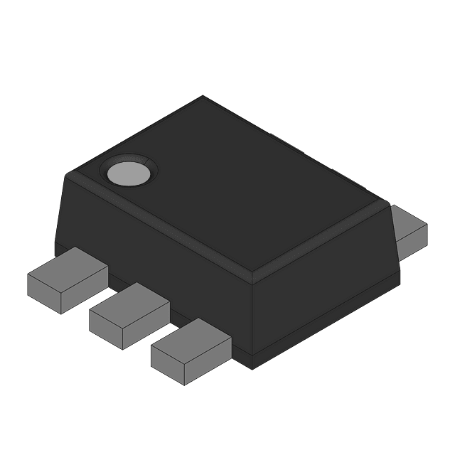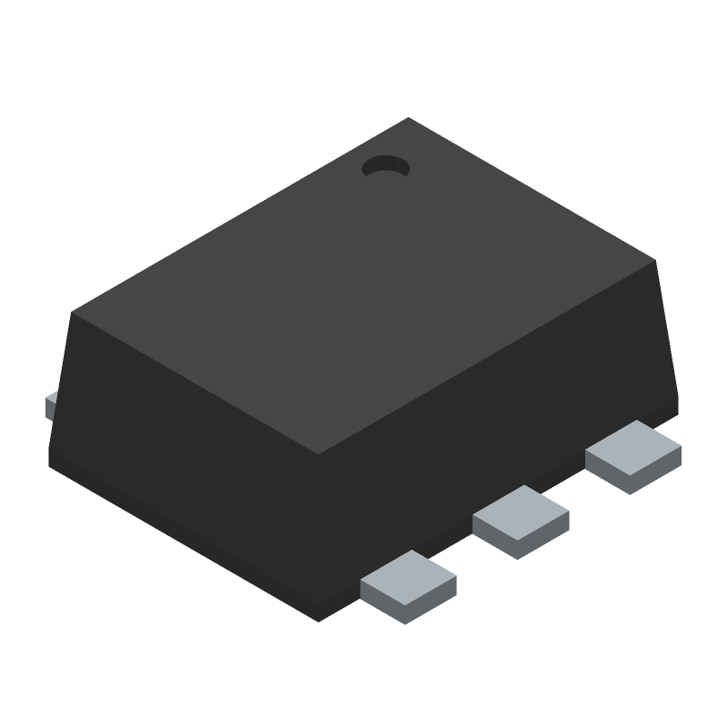
N-Channel Enhancement Mode Field Effect Transistor, dual element configuration. Features 60V Drain to Source Breakdown Voltage (Vdss) and 280mA Continuous Drain Current (ID). Offers a maximum Drain-source On Resistance (Rds On) of 7.5 Ohms. Operates within a temperature range of -55°C to 150°C. Surface mountable in a SOT-563 package, supplied on a 3000-piece tape and reel. RoHS compliant with tin-matte contact plating.
Onsemi 2N7002V technical specifications.
| Package/Case | SOT-563 |
| Contact Plating | Tin, Matte |
| Continuous Drain Current (ID) | 280mA |
| Drain to Source Breakdown Voltage | 60V |
| Drain to Source Resistance | 7.5R |
| Drain to Source Voltage (Vdss) | 60V |
| Drain-source On Resistance-Max | 7.5R |
| Element Configuration | Dual |
| FET Type | 2 N-Channel |
| Gate to Source Voltage (Vgs) | 20V |
| Height | 0.6mm |
| Input Capacitance | 50pF |
| Lead Free | Lead Free |
| Length | 1.7mm |
| Max Operating Temperature | 150°C |
| Min Operating Temperature | -55°C |
| Max Power Dissipation | 250mW |
| Mount | Surface Mount |
| Nominal Vgs | 1.76V |
| Number of Elements | 2 |
| Package Quantity | 3000 |
| Packaging | Tape and Reel |
| Polarity | N-CHANNEL |
| Power Dissipation | 250mW |
| Radiation Hardening | No |
| Rds On Max | 7.5R |
| Reach SVHC Compliant | No |
| RoHS Compliant | Yes |
| Threshold Voltage | 1.76V |
| Turn-Off Delay Time | 12.5ns |
| Turn-On Delay Time | 5.85ns |
| Weight | 0.032g |
| Width | 1.2mm |
| RoHS | Compliant |
No datasheet is available for this part.