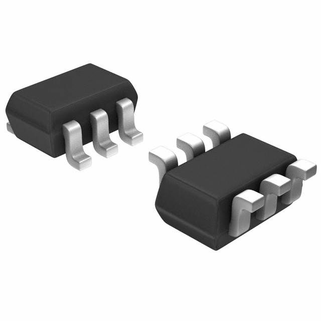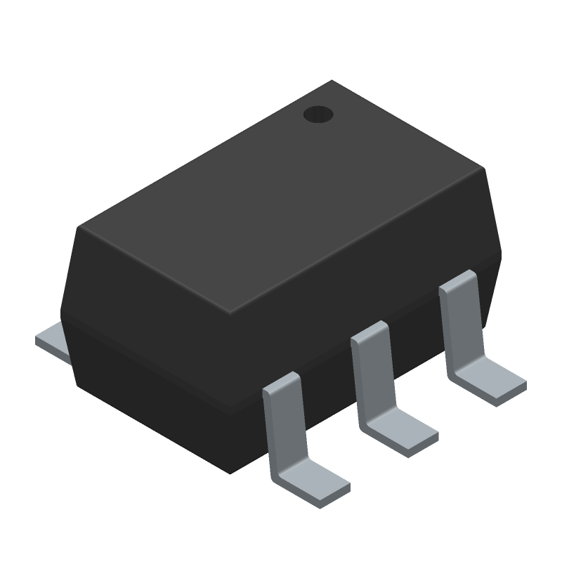
Dual P-Channel JFET with -25V Drain to Source Breakdown Voltage and 410mA Continuous Drain Current. Features 1.1 Ohm maximum Drain-source On Resistance and 300mW maximum Power Dissipation. Operates from -55°C to 150°C, with 7ns Turn-On Delay Time and 8ns Fall Time. Packaged in SC for surface mounting, supplied on a 3000-piece tape and reel.
Checking distributor stock and pricing after the page loads.
Sign in to ask questions about the Onsemi FDG6304P datasheet using AI. Get instant answers about specifications, features, and technical details, ideal for finding information in larger documents.
Sign In to ChatWidest selection of semiconductors and electronic components in stock and ready to ship ™
| Package/Case | SC |
| Continuous Drain Current (ID) | 410mA |
| Current Rating | -410mA |
| Drain to Source Breakdown Voltage | -25V |
| Drain to Source Resistance | 1.1R |
| Drain to Source Voltage (Vdss) | 25V |
| Drain-source On Resistance-Max | 1.1R |
| Dual Supply Voltage | -25V |
| Element Configuration | Dual |
| Fall Time | 8ns |
| Gate to Source Voltage (Vgs) | -8V |
| Input Capacitance | 62pF |
| Lead Free | Lead Free |
| Max Operating Temperature | 150°C |
| Min Operating Temperature | -55°C |
| Max Power Dissipation | 300mW |
| Mount | Surface Mount |
| Nominal Vgs | -820mV |
| Number of Elements | 2 |
| Package Quantity | 3000 |
| Packaging | Tape and Reel |
| Polarity | P-CHANNEL |
| Power Dissipation | 300mW |
| Radiation Hardening | No |
| Rds On Max | 1.1R |
| Reach SVHC Compliant | No |
| RoHS Compliant | Yes |
| Termination | SMD/SMT |
| Threshold Voltage | -820mV |
| Turn-Off Delay Time | 55ns |
| Turn-On Delay Time | 7ns |
| DC Rated Voltage | -25V |
| Weight | 0.028g |
| RoHS | Compliant |
Download the complete datasheet for Onsemi FDG6304P to view detailed technical specifications.
The embedded preview will load automatically when this section scrolls into view.