N-channel enhancement mode power MOSFET featuring a dual configuration in an 8-pin DFN EP package. This surface-mount component offers a 30V drain-source voltage and supports continuous drain currents of 12A and 17A. Key specifications include a low drain-source on-resistance of 7.5mOhm and 5mOhm at 10V, with typical gate charge values of 20nC and 33nC at 10V. Operating temperature range is -55°C to 150°C.
Checking distributor stock and pricing after the page loads.
Sign in to ask questions about the Onsemi FDMS7602S datasheet using AI. Get instant answers about specifications, features, and technical details, ideal for finding information in larger documents.
Sign In to ChatWidest selection of semiconductors and electronic components in stock and ready to ship ™
| Basic Package Type | Non-Lead-Frame SMT |
| Package Family Name | DFN |
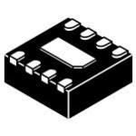
| Package/Case | DFN EP |
| Package Description | Dual Flat Package No Lead, Exposed Pad |
| Lead Shape | No Lead |
| Pin Count | 8 |
| PCB | 8 |
| Package Length (mm) | 5 |
| Package Width (mm) | 6 |
| Package Height (mm) | 0.5 |
| Seated Plane Height (mm) | 0.75 |
| Pin Pitch (mm) | 1.27 |
| Package Material | Plastic |
| Mounting | Surface Mount |
| Configuration | Dual |
| Category | Power MOSFET |
| Channel Mode | Enhancement |
| Channel Type | N |
| Number of Elements per Chip | 2 |
| Process Technology | TMOS |
| Maximum Drain Source Voltage | 30V |
| Maximum Gate Source Voltage | ±20V |
| Maximum Continuous Drain Current | 12@Q 1|17@Q 2A |
| Material | Si |
| Maximum Drain Source Resistance | 7.5@10V@Q 1|5@10V@Q 2mOhm |
| Typical Gate Charge @ Vgs | 20@10V|[email protected]@Q 1|33@10V|[email protected]@Q 2nC |
| Typical Gate Charge @ 10V | 20@Q 1|33@Q 2nC |
| Typical Input Capacitance @ Vds | 1315@15V@Q 1|2020@15V@Q 2pF |
| Maximum Power Dissipation | 2200@Q 1|2500@Q 2mW |
| Min Operating Temperature | -55°C |
| Max Operating Temperature | 150°C |
| Cage Code | 5V1P1 |
| EU RoHS | Yes |
| HTS Code | 8541290095 |
| Schedule B | 8541290080 |
| ECCN | EAR99 |
| Automotive | No |
| AEC Qualified | No |
| PPAP | No |
| Radiation Hardening | No |
| RoHS Versions | 2011/65/EU, 2015/863 |
Download the complete datasheet for Onsemi FDMS7602S to view detailed technical specifications.
The embedded preview will load automatically when this section scrolls into view.