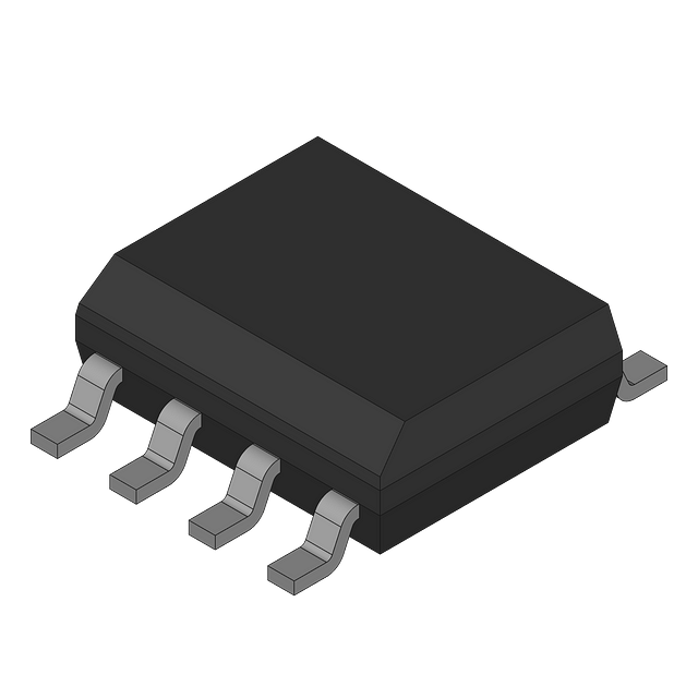
Dual N-Channel Power MOSFET, surface mountable in an SOIC package. Features a 30V Drain to Source Breakdown Voltage and 30mΩ Drain to Source Resistance at a nominal Vgs of 670mV. Continuous drain current is rated at 5.5A, with a maximum power dissipation of 2W. Operates across a temperature range of -55°C to 150°C, offering a fall time of 13ns and turn-off delay of 42ns.
Sign in to ask questions about the Onsemi FDS8926A datasheet using AI. Get instant answers about specifications, features, and technical details, ideal for finding information in larger documents.
Sign In to ChatWidest selection of semiconductors and electronic components in stock and ready to ship ™
Onsemi FDS8926A technical specifications.
| Package/Case | SOIC |
| Continuous Drain Current (ID) | 5.5A |
| Current Rating | 5.5A |
| Drain to Source Breakdown Voltage | 30V |
| Drain to Source Resistance | 30mR |
| Drain to Source Voltage (Vdss) | 30V |
| Dual Supply Voltage | 30V |
| Element Configuration | Dual |
| Fall Time | 13ns |
| FET Type | 2 N-Channel |
| Gate to Source Voltage (Vgs) | 8V |
| Input Capacitance | 900pF |
| Lead Free | Lead Free |
| Max Operating Temperature | 150°C |
| Min Operating Temperature | -55°C |
| Max Power Dissipation | 900mW |
| Mount | Surface Mount |
| Nominal Vgs | 670mV |
| Number of Elements | 2 |
| Package Quantity | 1 |
| Packaging | Tape and Reel |
| Polarity | N-CHANNEL |
| Power Dissipation | 2W |
| Radiation Hardening | No |
| Rds On Max | 30mR |
| Reach SVHC Compliant | No |
| Termination | SMD/SMT |
| Turn-Off Delay Time | 42ns |
| DC Rated Voltage | 30V |
| Weight | 0.2304g |
| RoHS | Not CompliantNo |
Download the complete datasheet for Onsemi FDS8926A to view detailed technical specifications.
The embedded preview will load automatically when this section scrolls into view.
