N-Channel Power MOSFET featuring a 250V drain-source voltage and 4.4A continuous drain current. This UniFET™ device offers a low 1.1Ω drain-source resistance and is housed in a TO-251-3 IPAK package for through-hole mounting. Key switching characteristics include a 34ns fall time, 7ns turn-off delay, and 10ns turn-on delay, with an input capacitance of 250pF. Maximum power dissipation is rated at 50W, operating within a temperature range of -55°C to 150°C.
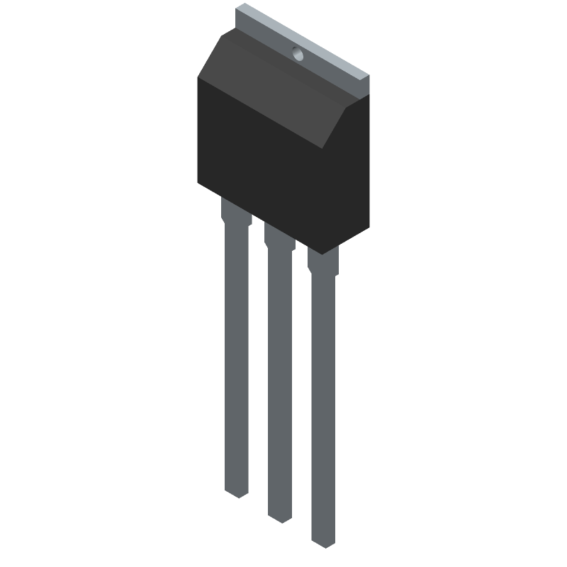
PackageTO-251-3
MountingThrough Hole
PolarityN-CHANNEL
Quick Jump:
Chat with Datasheet
Sponsored by
Sign in to ask questions about the Onsemi FDU6N25 datasheet using AI. Get instant answers about specifications, features, and technical details, ideal for finding information in larger documents.
Sign In to ChatWidest selection of semiconductors and electronic components in stock and ready to ship ™
Technical Specifications
Onsemi FDU6N25 technical specifications.
General
| Package/Case | TO-251-3 |
| Continuous Drain Current (ID) | 4.4A |
| Drain to Source Resistance | 1.1R |
| Drain to Source Voltage (Vdss) | 250V |
| Element Configuration | Single |
| Fall Time | 34ns |
| Gate to Source Voltage (Vgs) | 30V |
| Height | 7.57mm |
| Input Capacitance | 250pF |
| Length | 6.8mm |
| Max Operating Temperature | 150°C |
| Min Operating Temperature | -55°C |
| Max Power Dissipation | 50W |
| Mount | Through Hole |
| Package Quantity | 70 |
| Packaging | Rail/Tube |
| Polarity | N-CHANNEL |
| Radiation Hardening | No |
| Rds On Max | 1.1R |
| RoHS Compliant | Yes |
| Series | UniFET™ |
| Turn-Off Delay Time | 7ns |
| Turn-On Delay Time | 10ns |
| Weight | 0.539g |
| Width | 2.5mm |
Compliance
| RoHS | Compliant |
Datasheet
Onsemi FDU6N25 Datasheet
Download the complete datasheet for Onsemi FDU6N25 to view detailed technical specifications.
The embedded preview will load automatically when this section scrolls into view.