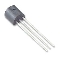
N-channel Junction Field-Effect Transistor (JFET) designed for through-hole mounting in a TO-92 package. Features a continuous drain current of 5mA, a drain-to-source voltage rating of 35V, and a gate-to-source voltage of -35V. Offers a drain-to-source resistance of 50 Ohms and a maximum power dissipation of 625mW. Operates within a temperature range of -55°C to 150°C and is RoHS compliant.
PackageTO-92
Voltage35V
Current Rating50mA
MountingThrough Hole
Quick Jump:
Chat with Datasheet
Sponsored by
Sign in to ask questions about the Onsemi J112 datasheet using AI. Get instant answers about specifications, features, and technical details, ideal for finding information in larger documents.
Sign In to ChatWidest selection of semiconductors and electronic components in stock and ready to ship ™
Technical Specifications
Onsemi J112 technical specifications.
General
| Package/Case | TO-92 |
| Continuous Drain Current (ID) | 5mA |
| Current Rating | 50mA |
| Drain to Source Resistance | 50R |
| Drain to Source Voltage (Vdss) | 35V |
| Gate to Source Voltage (Vgs) | -35V |
| Height | 5.33mm |
| Lead Free | Lead Free |
| Length | 5.2mm |
| Max Operating Temperature | 150°C |
| Min Operating Temperature | -55°C |
| Max Power Dissipation | 625mW |
| Mount | Through Hole |
| Package Quantity | 1000 |
| Packaging | Bulk |
| Polarity | N-CHANNEL |
| Power Dissipation | 350mW |
| Radiation Hardening | No |
| Reach SVHC Compliant | No |
| RoHS Compliant | Yes |
| Voltage | 35V |
| DC Rated Voltage | 35V |
| Weight | 0.00709oz |
| Width | 4.19mm |
Compliance
| RoHS | Compliant |
Datasheet
Onsemi J112 Datasheet
Download the complete datasheet for Onsemi J112 to view detailed technical specifications.
The embedded preview will load automatically when this section scrolls into view.
Product Images
