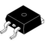
N-channel enhancement mode power MOSFET, 50V drain-source voltage, 75A continuous drain current, and 9.5mΩ maximum drain-source on-resistance at 10V. Features a 3-pin D2PAK (TO-263) surface-mount package with gull-wing leads, measuring 10.29mm max length and 9.65mm max width. Typical gate charge is 71nC at 10V, with 2600pF input capacitance at 25V. Maximum power dissipation is 2500mW, operating temperature range from -55°C to 150°C.
PackageD2PAK
MountingSurface Mount
Quick Jump:
Technical Specifications
Onsemi MTB75N05HDT4 technical specifications.
General
| Basic Package Type | Lead-Frame SMT |
| Package Family Name | TO-263 |
| Package/Case | D2PAK |
| Package Description | Double Deca Watt Package |
| Lead Shape | Gull-wing |
| Pin Count | 3 |
| PCB | 2 |
| Tab | Tab |
| Package Length (mm) | 10.29(Max) |
| Package Width (mm) | 9.65(Max) |
| Package Height (mm) | 4.83(Max) |
| Seated Plane Height (mm) | 4.83(Max) |
| Pin Pitch (mm) | 2.54 |
| Package Material | Plastic |
| Mounting | Surface Mount |
| Jedec | TS-005AA |
| Configuration | Single |
| Category | Power MOSFET |
| Channel Mode | Enhancement |
| Channel Type | N |
| Number of Elements per Chip | 1 |
| Maximum Drain Source Voltage | 50V |
| Maximum Gate Source Voltage | ±20V |
| Maximum Continuous Drain Current | 75A |
| Maximum Drain Source Resistance | 9.5@10VmOhm |
| Typical Gate Charge @ Vgs | 71@10VnC |
| Typical Gate Charge @ 10V | 71nC |
| Typical Input Capacitance @ Vds | 2600@25VpF |
| Maximum Power Dissipation | 2500mW |
| Min Operating Temperature | -55°C |
| Max Operating Temperature | 150°C |
Compliance
| Cage Code | 5V1P1 |
| EU RoHS | No |
| HTS Code | 8541290095 |
| Schedule B | 8541290080 |
| ECCN | EAR99 |
| Automotive | No |
| AEC Qualified | No |
| PPAP | No |
| Radiation Hardening | No |
| RoHS Versions | 2011/65/EU, 2015/863 |
Datasheet
Onsemi MTB75N05HDT4 Datasheet
Download the complete datasheet for Onsemi MTB75N05HDT4 to view detailed technical specifications.
This datasheet cannot be embedded due to technical restrictions.