N-channel enhancement mode power MOSFET, 60V drain-source voltage, 12A continuous drain current. Features 180mOhm maximum drain-source resistance at 5V Vgs. Surface mount DPAK (TO-252AA) package with 3 pins and gull-wing leads. Maximum power dissipation of 3900mW, operating temperature range of -55°C to 175°C.
Checking distributor stock and pricing after the page loads.
Sign in to ask questions about the Onsemi MTD3055VL datasheet using AI. Get instant answers about specifications, features, and technical details, ideal for finding information in larger documents.
Sign In to ChatWidest selection of semiconductors and electronic components in stock and ready to ship ™
| Basic Package Type | Lead-Frame SMT |
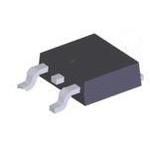
| Package Family Name | TO-252 |
| Package/Case | DPAK |
| Package Description | Deca Watt Package |
| Lead Shape | Gull-wing |
| Pin Count | 3 |
| PCB | 2 |
| Tab | Tab |
| Package Length (mm) | 6.73(Max) |
| Package Width (mm) | 6.22(Max) |
| Package Height (mm) | 2.39(Max) |
| Seated Plane Height (mm) | 2.52(Max) |
| Pin Pitch (mm) | 2.29 |
| Package Material | Plastic |
| Mounting | Surface Mount |
| Package Orientation | Yes |
| Package Orientation Marking Type | Beveled Edge |
| Jedec | TO-252AA |
| Configuration | Single |
| Category | Power MOSFET |
| Channel Mode | Enhancement |
| Channel Type | N |
| Number of Elements per Chip | 1 |
| Maximum Drain Source Voltage | 60V |
| Maximum Gate Source Voltage | ±20V |
| Maximum Continuous Drain Current | 12A |
| Maximum Gate Threshold Voltage | 2V |
| Maximum Drain Source Resistance | 180@5VmOhm |
| Typical Gate Charge @ Vgs | 10(Max)@5VnC |
| Typical Input Capacitance @ Vds | 570(Max)@25VpF |
| Maximum Power Dissipation | 3900mW |
| Min Operating Temperature | -55°C |
| Max Operating Temperature | 175°C |
| Typical Output Capacitance | 160(Max)pF |
| Cage Code | 5V1P1 |
| EU RoHS | Yes with Exemption |
| HTS Code | 8541290095 |
| Schedule B | 8541290080 |
| ECCN | EAR99 |
| Automotive | No |
| AEC Qualified | No |
| PPAP | No |
| Radiation Hardening | No |
| RoHS Versions | 2011/65/EU, 2015/863 |
Download the complete datasheet for Onsemi MTD3055VL to view detailed technical specifications.
The embedded preview will load automatically when this section scrolls into view.
These are design resources that include the Onsemi MTD3055VL
Product discontinuance notice from onsemi for various MOSFETs and transistors produced at the Tower Jazz fab, providing end-of-life dates and potential replacement parts.
Immediate product discontinuance notice from onsemi for various MOSFETs and discrete components produced at the Tower fab, effective December 24, 2021.