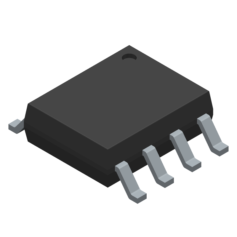
Automotive-grade Zero Delay Buffer featuring a single-ended clock input and five outputs. This integrated circuit operates with a nominal supply voltage of 3.3V, ranging from 3V to 3.6V, and consumes a maximum supply current of 50mA. It supports frequencies up to 133MHz and includes a Phase-Locked Loop (PLL) for precise clock distribution. Packaged in an 8-pin SOIC surface-mount case, this component is halogen-free, lead-free, and RoHS compliant, with an operating temperature range of -40°C to 85°C.
Checking distributor stock and pricing after the page loads.
| Package/Case | SOIC |
| Frequency | 133MHz |
| Halogen Free | Halogen Free |
| Height | 1.5mm |
| Input | Clock |
| Lead Free | Lead Free |
| Length | 5mm |
| Max Frequency | 133MHz |
| Max Operating Temperature | 85°C |
| Min Operating Temperature | -40°C |
| Max Supply Current | 50mA |
| Max Supply Voltage | 3.6V |
| Min Supply Voltage | 3V |
| Mount | Surface Mount |
| Number of Circuits | 1 |
| Number of Elements | 1 |
| Number of Outputs | 5 |
| Operating Supply Voltage | 3.3V |
| Package Quantity | 1 |
| Packaging | Tape and Reel |
| PLL | Yes |
| Radiation Hardening | No |
| Reach SVHC Compliant | No |
| RoHS Compliant | Yes |
| Supply Current | 50mA |
| Supply Voltage-Nom | 3.3V |
| Width | 4mm |
| RoHS | Compliant |
