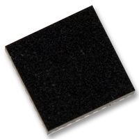
12-output LVCMOS/LVTTL clock buffer, operating up to 250MHz with a maximum duty cycle of 55%. This surface mount component features a 1.8V to 3.3V supply voltage range and a low supply current of 150uA. Housed in a 5x5mm QFN package with a 0.95mm height, it offers a propagation delay of 4.2ns. Designed for optimal performance, it is RoHS compliant and operates within a temperature range of -40°C to 85°C.
Checking distributor stock and pricing after the page loads.
| Package/Case | QFN |
| Frequency | 250MHz |
| Height | 0.95mm |
| Input | LVTTL |
| Lead Free | Lead Free |
| Length | 5mm |
| Max Duty Cycle | 55% |
| Max Frequency | 250MHz |
| Max Operating Temperature | 85°C |
| Min Operating Temperature | -40°C |
| Max Supply Current | 150uA |
| Max Supply Voltage | 3.3V |
| Min Supply Voltage | 1.8V |
| Mount | Surface Mount |
| Number of Circuits | 1 |
| Number of Outputs | 12 |
| Operating Supply Current | 150uA |
| Package Quantity | 74 |
| Packaging | Rail/Tube |
| Propagation Delay | 4.2ns |
| Reach SVHC Compliant | No |
| RoHS Compliant | Yes |
| Weight | 0.006653oz |
| Width | 5mm |
| RoHS | Compliant |
