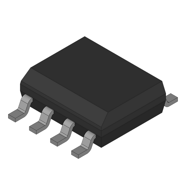
N- and P-channel dual JFET transistor in SOIC package for surface mount applications. Features 30V drain-to-source breakdown voltage, 4.8A continuous drain current, and 35mΩ drain-to-source resistance. Operates across a wide temperature range from -55°C to 150°C with a maximum power dissipation of 2.5W. Includes 19ns fall time and 40ns turn-off delay time, with 720pF input capacitance. Lead-free and supplied on tape and reel.
Checking distributor stock and pricing after the page loads.
Sign in to ask questions about the Onsemi NDS8858H datasheet using AI. Get instant answers about specifications, features, and technical details, ideal for finding information in larger documents.
Sign In to ChatWidest selection of semiconductors and electronic components in stock and ready to ship ™
| Package/Case | SOIC |
| Continuous Drain Current (ID) | 4.8A |
| Current Rating | 4.8A |
| Drain to Source Breakdown Voltage | 30V |
| Drain to Source Resistance | 35mR |
| Drain to Source Voltage (Vdss) | 30V |
| Fall Time | 19ns |
| FET Type | N and P-Channel |
| Gate to Source Voltage (Vgs) | 20V |
| Input Capacitance | 720pF |
| Lead Free | Lead Free |
| Max Operating Temperature | 150°C |
| Min Operating Temperature | -55°C |
| Max Power Dissipation | 1W |
| Mount | Surface Mount |
| Number of Elements | 2 |
| Package Quantity | 2500 |
| Packaging | Tape and Reel |
| Polarity | P-CHANNEL |
| Power Dissipation | 2.5W |
| Radiation Hardening | No |
| Rds On Max | 35mR |
| Turn-Off Delay Time | 40ns |
| Weight | 0.2304g |
| RoHS | Not CompliantNo |
Download the complete datasheet for Onsemi NDS8858H to view detailed technical specifications.
The embedded preview will load automatically when this section scrolls into view.