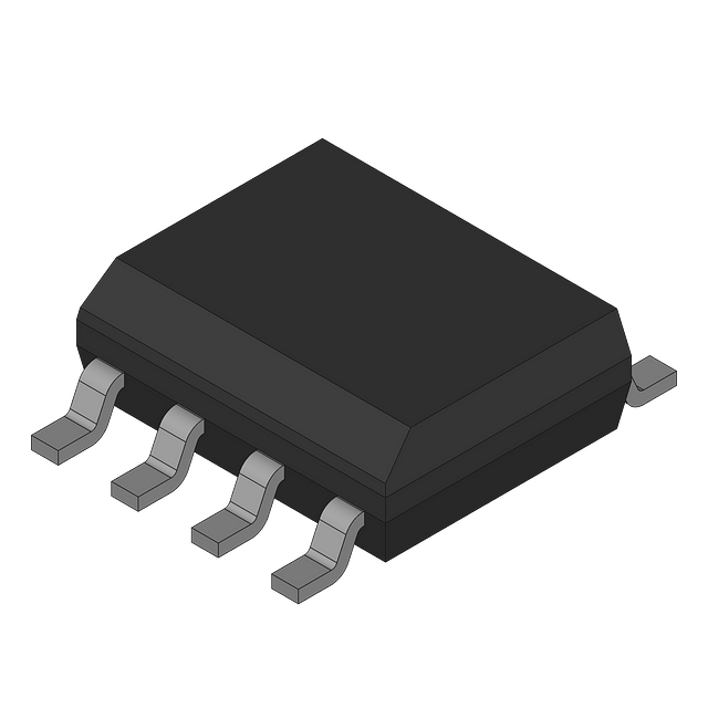
P-channel, dual-element silicon JFET for surface mounting. Features a continuous drain current of 4A, drain-source breakdown voltage of -30V, and a maximum drain-source on-resistance of 65mR. Operates with a gate-to-source voltage up to 20V and a nominal threshold voltage of -1.6V. Maximum power dissipation is 900mW, with a maximum operating temperature of 150°C. Packaged in SOIC for tape and reel distribution.
Checking distributor stock and pricing after the page loads.
Sign in to ask questions about the Onsemi NDS8947 datasheet using AI. Get instant answers about specifications, features, and technical details, ideal for finding information in larger documents.
Sign In to ChatWidest selection of semiconductors and electronic components in stock and ready to ship ™
| Package/Case | SOIC |
| Continuous Drain Current (ID) | 4A |
| Current Rating | -4A |
| Drain to Source Breakdown Voltage | -30V |
| Drain to Source Resistance | 65mR |
| Drain to Source Voltage (Vdss) | 30V |
| Drain-source On Resistance-Max | 65mR |
| Dual Supply Voltage | -30V |
| Element Configuration | Dual |
| Fall Time | 19ns |
| Gate to Source Voltage (Vgs) | 20V |
| Input Capacitance | 690pF |
| Lead Free | Lead Free |
| Max Operating Temperature | 150°C |
| Min Operating Temperature | -55°C |
| Max Power Dissipation | 900mW |
| Mount | Surface Mount |
| Nominal Vgs | -1.6V |
| Package Quantity | 2500 |
| Packaging | Tape and Reel |
| Polarity | P-CHANNEL |
| Power Dissipation | 2W |
| Radiation Hardening | No |
| Rds On Max | 65mR |
| Reach SVHC Compliant | No |
| Row Spacing | 6.3mm |
| Threshold Voltage | -1.6V |
| Turn-Off Delay Time | 40ns |
| Turn-On Delay Time | 9ns |
| DC Rated Voltage | -30V |
| Weight | 0.2304g |
| Width | 4.05mm |
| RoHS | Not CompliantNo |
Download the complete datasheet for Onsemi NDS8947 to view detailed technical specifications.
The embedded preview will load automatically when this section scrolls into view.
These are design resources that include the Onsemi NDS8947
Product Discontinuation Notice (PDN) P21AA from Fairchild Semiconductor listing end-of-life parts including bridge rectifiers, logic ICs, MOSFETs, and PWM controllers.
