Single P-Channel Power MOSFET featuring a -20V drain-source breakdown voltage and a continuous drain current of 2.2A. This MOSFET offers a low drain-source on-resistance of 65mΩ at a gate-source voltage of 12V. Designed for efficient power switching, it operates within a temperature range of -55°C to 150°C and is packaged in a compact TSOP. Key performance characteristics include a 30ns turn-on delay and a 31ns fall time, with a maximum power dissipation of 500mW.
Checking distributor stock and pricing after the page loads.
Sign in to ask questions about the Onsemi NTGS3443T1G datasheet using AI. Get instant answers about specifications, features, and technical details, ideal for finding information in larger documents.
Sign In to ChatWidest selection of semiconductors and electronic components in stock and ready to ship ™
Onsemi NTGS3443T1G technical specifications.
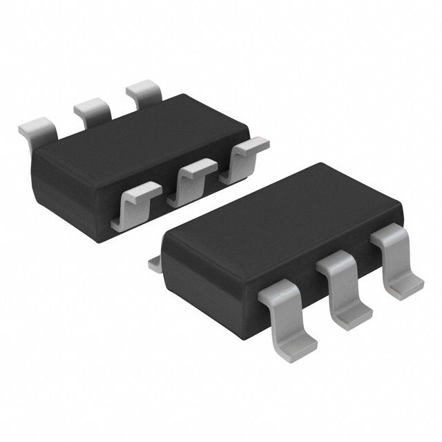
| Package/Case | TSOP |
| Continuous Drain Current (ID) | 2.2A |
| Current Rating | -2A |
| Drain to Source Breakdown Voltage | -20V |
| Drain to Source Resistance | 65mR |
| Drain to Source Voltage (Vdss) | 20V |
| Drain-source On Resistance-Max | 65MR |
| Element Configuration | Single |
| Fall Time | 31ns |
| Gate to Source Voltage (Vgs) | 12V |
| Height | 0.039inch |
| Input Capacitance | 565pF |
| Lead Free | Lead Free |
| Length | 0.122inch |
| Max Operating Temperature | 150°C |
| Min Operating Temperature | -55°C |
| Max Power Dissipation | 500mW |
| Number of Elements | 1 |
| Package Quantity | 1 |
| Packaging | Tape and Reel |
| Polarity | P-CHANNEL |
| Polarization | P |
| Power Dissipation | 2W |
| Radiation Hardening | No |
| Rds On Max | 65mR |
| Reach SVHC Compliant | No |
| RoHS Compliant | Yes |
| Threshold Voltage | -950mV |
| Turn-Off Delay Time | 30ns |
| Turn-On Delay Time | 10ns |
| DC Rated Voltage | -20V |
| Width | 0.067inch |
| RoHS | Compliant |
Download the complete datasheet for Onsemi NTGS3443T1G to view detailed technical specifications.
The embedded preview will load automatically when this section scrolls into view.