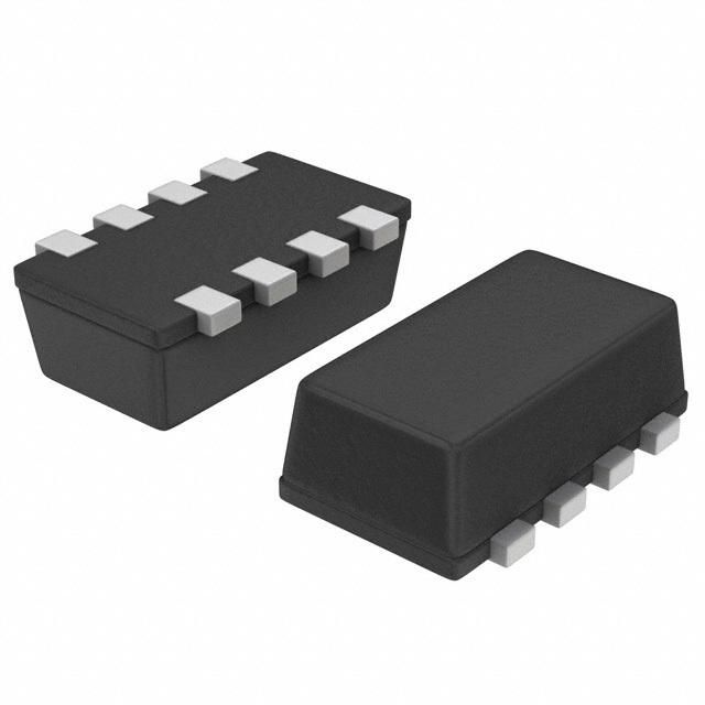
Dual N- and P-Channel Complementary Power MOSFET, featuring a 20V Drain to Source Voltage (Vdss) and 3.2A Continuous Drain Current (ID). This SMD/SMT packaged MOSFET offers a low Drain to Source Resistance (Rds On) of 64mR at a Gate to Source Voltage (Vgs) of 8V. With a maximum power dissipation of 1.1W and operating temperatures from -55°C to 150°C, it is suitable for various electronic applications. The component is RoHS compliant and supplied in a 3000-piece tape and reel.
Checking distributor stock and pricing after the page loads.
Onsemi NTHD3100CT1G technical specifications.
| Package/Case | SMD/SMT |
| Continuous Drain Current (ID) | 3.2A |
| Current Rating | 2.9A |
| Drain to Source Breakdown Voltage | -20V |
| Drain to Source Resistance | 64mR |
| Drain to Source Voltage (Vdss) | 20V |
| Element Configuration | Dual |
| Fall Time | 11.7ns |
| FET Type | N and P-Channel |
| Gate to Source Voltage (Vgs) | 8V |
| Height | 0.039inch |
| Input Capacitance | 165pF |
| Lead Free | Lead Free |
| Length | 0.122inch |
| Max Operating Temperature | 150°C |
| Min Operating Temperature | -55°C |
| Max Power Dissipation | 1.1W |
| Number of Elements | 2 |
| Package Quantity | 3000 |
| Packaging | Tape and Reel |
| Polarity | P-CHANNEL |
| Power Dissipation | 1.1W |
| Radiation Hardening | No |
| Rds On Max | 80mR |
| Reach SVHC Compliant | No |
| RoHS Compliant | Yes |
| Threshold Voltage | -1.5V |
| Turn-Off Delay Time | 16ns |
| Turn-On Delay Time | 6.3ns |
| DC Rated Voltage | 20V |
| Width | 0.067inch |
| RoHS | Compliant |
No datasheet is available for this part.
