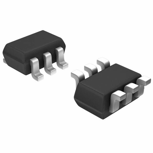
High-side power switch featuring dual N-channel and P-channel FETs in a compact SOT-363-6 package. Offers a continuous drain current of 1.3A with a low on-resistance of 130mR (max). Operates with a gate-to-source voltage of 1V and a threshold voltage of 1V, supporting a drain-to-source breakdown voltage of -8V. This RoHS compliant component is designed for efficient power management with a maximum power dissipation of 400mW.
Sign in to ask questions about the Onsemi NTJD1155LT1G datasheet using AI. Get instant answers about specifications, features, and technical details, ideal for finding information in larger documents.
Sign In to ChatWidest selection of semiconductors and electronic components in stock and ready to ship ™
Onsemi NTJD1155LT1G technical specifications.
| Package/Case | SOT-363-6 |
| Continuous Drain Current (ID) | 1.3A |
| Current Rating | 630mA |
| Drain to Source Breakdown Voltage | -8V |
| Drain to Source Resistance | 260mR |
| Drain-source On Resistance-Max | 130mR |
| Element Configuration | Dual |
| FET Type | N and P-Channel |
| Gate to Source Voltage (Vgs) | 1V |
| Height | 1mm |
| Lead Free | Lead Free |
| Length | 2.2mm |
| Max Operating Temperature | 150°C |
| Min Operating Temperature | -55°C |
| Max Power Dissipation | 400mW |
| Number of Channels | 1 |
| Number of Elements | 2 |
| Package Quantity | 3000 |
| Packaging | Tape and Reel |
| Polarity | P-CHANNEL |
| Power Dissipation | 400mW |
| Radiation Hardening | No |
| Rds On Max | 175mR |
| Reach SVHC Compliant | No |
| RoHS Compliant | Yes |
| Threshold Voltage | 1V |
| Width | 1.35mm |
| RoHS | Compliant |
Download the complete datasheet for Onsemi NTJD1155LT1G to view detailed technical specifications.
The embedded preview will load automatically when this section scrolls into view.