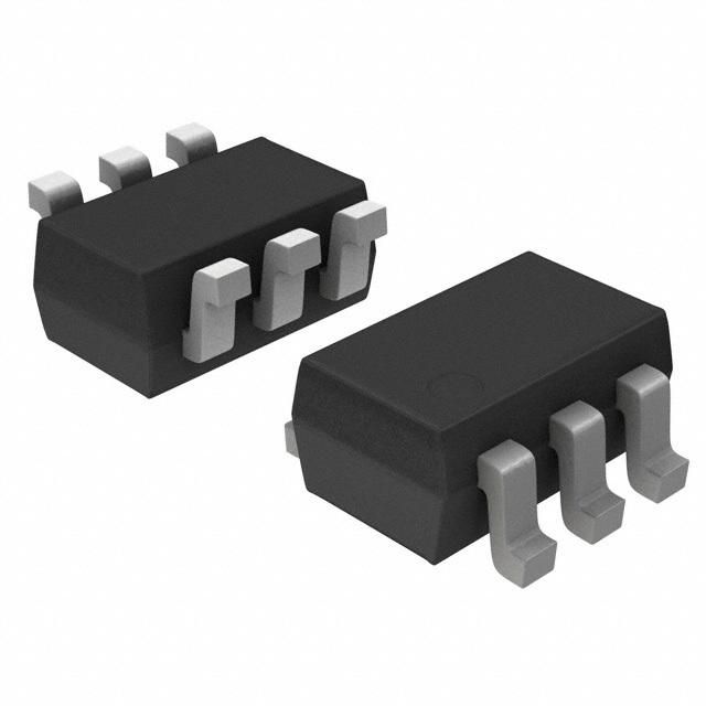
Dual N and P-Channel JFET transistor in a SOT-363-6 package. Features a continuous drain current of 775mA and a drain-source breakdown voltage of -8V. Offers a drain-source on resistance of 220mR (max) and a gate-to-source voltage of 8V. Operates within a temperature range of -55°C to 150°C with a maximum power dissipation of 270mW. Packaged on a 3000-piece tape and reel, this component is lead-free and RoHS compliant.
Checking distributor stock and pricing after the page loads.
Onsemi NTJD4105CT2G technical specifications.
| Package/Case | SOT-363-6 |
| Continuous Drain Current (ID) | 775mA |
| Current Rating | 630mA |
| Drain to Source Breakdown Voltage | -8V |
| Drain to Source Resistance | 220mR |
| Drain to Source Voltage (Vdss) | 8V |
| Drain-source On Resistance-Max | 220mR |
| Element Configuration | Dual |
| Fall Time | 36ns |
| FET Type | N and P-Channel |
| Gate to Source Voltage (Vgs) | 8V |
| Input Capacitance | 46pF |
| Lead Free | Lead Free |
| Max Operating Temperature | 150°C |
| Min Operating Temperature | -55°C |
| Max Power Dissipation | 270mW |
| Number of Elements | 2 |
| Package Quantity | 3000 |
| Packaging | Tape and Reel |
| Polarity | P-CHANNEL |
| Power Dissipation | 270mW |
| Radiation Hardening | No |
| Rds On Max | 375mR |
| RoHS Compliant | Yes |
| Turn-Off Delay Time | 50ns |
| RoHS | Compliant |
No datasheet is available for this part.