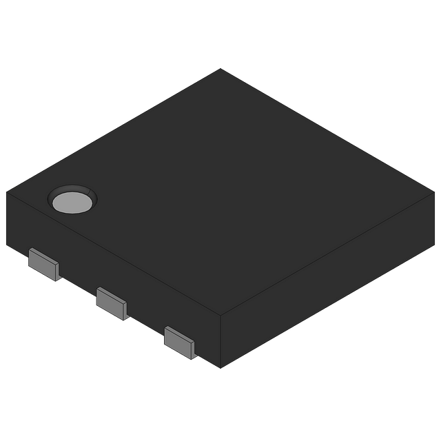
Dual N-Channel Power MOSFET featuring 20V Drain to Source Breakdown Voltage (Vdss) and a maximum continuous drain current (ID) of 4.3A. This component offers a low Drain-Source On Resistance (Rds On) of 60mR. Operating within a temperature range of -55°C to 150°C, it is housed in a compact DFN package with 3x3mm dimensions and 0.95mm pitch, supplied on a 3000-piece tape and reel. Key switching characteristics include a 7ns turn-on delay and 17.5ns fall time, with a maximum power dissipation of 1.74W.
Checking distributor stock and pricing after the page loads.
Sign in to ask questions about the Onsemi NTLGD3502NT2G datasheet using AI. Get instant answers about specifications, features, and technical details, ideal for finding information in larger documents.
Sign In to ChatWidest selection of semiconductors and electronic components in stock and ready to ship ™
Onsemi NTLGD3502NT2G technical specifications.
| Package/Case | DFN |
| Continuous Drain Current (ID) | 4.3A |
| Drain to Source Breakdown Voltage | 20V |
| Drain to Source Resistance | 60mR |
| Drain to Source Voltage (Vdss) | 20V |
| Drain-source On Resistance-Max | 60MR |
| Element Configuration | Dual |
| Fall Time | 17.5ns |
| FET Type | 2 N-Channel |
| Gate to Source Voltage (Vgs) | 20V |
| Input Capacitance | 480pF |
| Lead Free | Lead Free |
| Max Operating Temperature | 150°C |
| Min Operating Temperature | -55°C |
| Max Power Dissipation | 1.74W |
| Package Quantity | 3000 |
| Packaging | Tape and Reel |
| Polarity | N-CHANNEL |
| Power Dissipation | 1.74W |
| Radiation Hardening | No |
| Rds On Max | 60mR |
| RoHS Compliant | Yes |
| Turn-Off Delay Time | 8.6ns |
| Turn-On Delay Time | 7ns |
| RoHS | Compliant |
Download the complete datasheet for Onsemi NTLGD3502NT2G to view detailed technical specifications.
The embedded preview will load automatically when this section scrolls into view.