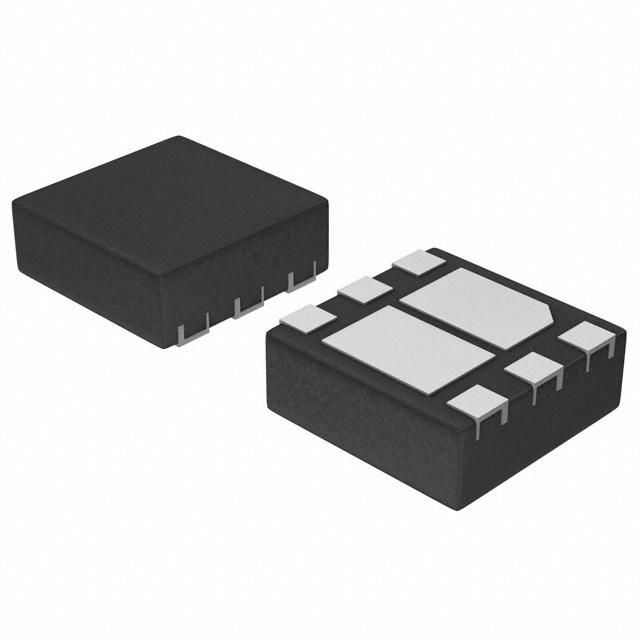
Dual P-Channel Power MOSFET featuring a -20V drain-source breakdown voltage and a continuous drain current of 3.3A. Offers a low drain-source on-resistance of 100mΩ at a 4.5V gate-source voltage. This MOSFET is housed in a compact 2x2mm WDFN6 package with a 0.65mm pitch, designed for efficient power management. Key electrical characteristics include a 6ns turn-on delay and 15ns fall time, with a maximum power dissipation of 710mW.
Sign in to ask questions about the Onsemi NTLJD3115PT1G datasheet using AI. Get instant answers about specifications, features, and technical details, ideal for finding information in larger documents.
Sign In to ChatWidest selection of semiconductors and electronic components in stock and ready to ship ™
Onsemi NTLJD3115PT1G technical specifications.
| Package/Case | DFN |
| Continuous Drain Current (ID) | 3.3A |
| Current Rating | -4.1A |
| Drain to Source Breakdown Voltage | 20V |
| Drain to Source Resistance | 100mR |
| Drain to Source Voltage (Vdss) | 20V |
| Drain-source On Resistance-Max | 100MR |
| Element Configuration | Dual |
| Fall Time | 15ns |
| Gate to Source Voltage (Vgs) | 8V |
| Height | 0.75mm |
| Input Capacitance | 531pF |
| Lead Free | Lead Free |
| Length | 2mm |
| Max Operating Temperature | 150°C |
| Min Operating Temperature | -55°C |
| Max Power Dissipation | 710mW |
| Number of Elements | 2 |
| Package Quantity | 3000 |
| Packaging | Tape and Reel |
| Polarity | P-CHANNEL |
| Power Dissipation | 1.5W |
| Radiation Hardening | No |
| Rds On Max | 100mR |
| RoHS Compliant | Yes |
| Turn-Off Delay Time | 19.8ns |
| Turn-On Delay Time | 6ns |
| DC Rated Voltage | -20V |
| Width | 2mm |
| RoHS | Compliant |
Download the complete datasheet for Onsemi NTLJD3115PT1G to view detailed technical specifications.
The embedded preview will load automatically when this section scrolls into view.