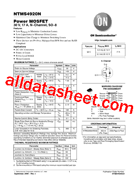
This device is an N-channel power MOSFET rated for 30 V drain-to-source voltage and up to 17 A drain current in an SO-8 package. It is designed for low on-resistance, low capacitance, and optimized gate charge to reduce conduction and switching losses. The datasheet lists maximum RDS(on) of 4.3 mΩ at 10 V gate drive and 5.7 mΩ at 4.5 V gate drive. Operating junction and storage temperature range is -55 °C to 150 °C. Typical applications include DC-DC converters, point-of-load circuits, power load switches, and motor controls. The device is identified as Pb-free, halogen-free/BFR-free, and RoHS compliant.
Checking distributor stock and pricing after the page loads.
Onsemi NTMS4920N technical specifications.
| Drain-to-Source Voltage | 30V |
| Gate-to-Source Voltage | ±20V |
| Continuous Drain Current | 17A |
| Pulsed Drain Current | 136A |
| Power Dissipation | 2.12W |
| Operating Junction Temperature | -55 to 150°C |
| Single Pulse Avalanche Energy | 162mJ |
| Gate Threshold Voltage | 1.5 to 3.0V |
| Drain-to-Source On Resistance @ VGS=10V | 4.3 maxmΩ |
| Drain-to-Source On Resistance @ VGS=4.5V | 5.7 maxmΩ |
| Input Capacitance | 4068pF |
| Output Capacitance | 1170pF |
| Reverse Transfer Capacitance | 41pF |
| Total Gate Charge @ VGS=4.5V | 26.3nC |
| Total Gate Charge @ VGS=10V | 58.9nC |
| Reverse Recovery Time | 50.3ns |
| Thermal Resistance Junction-to-Ambient | 85.5°C/W |
| Package | SO-8 |
| RoHS | Compliant |
| Pb-free | Yes |
| Halogen Free | Yes |
| Bfr Free | Yes |
