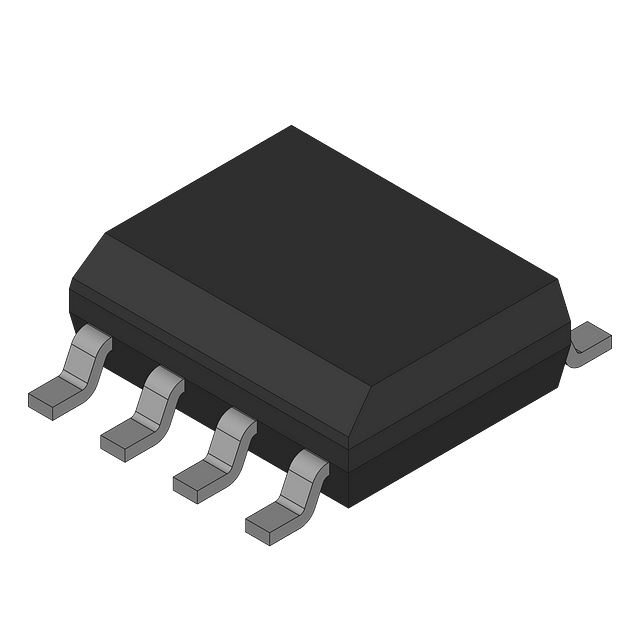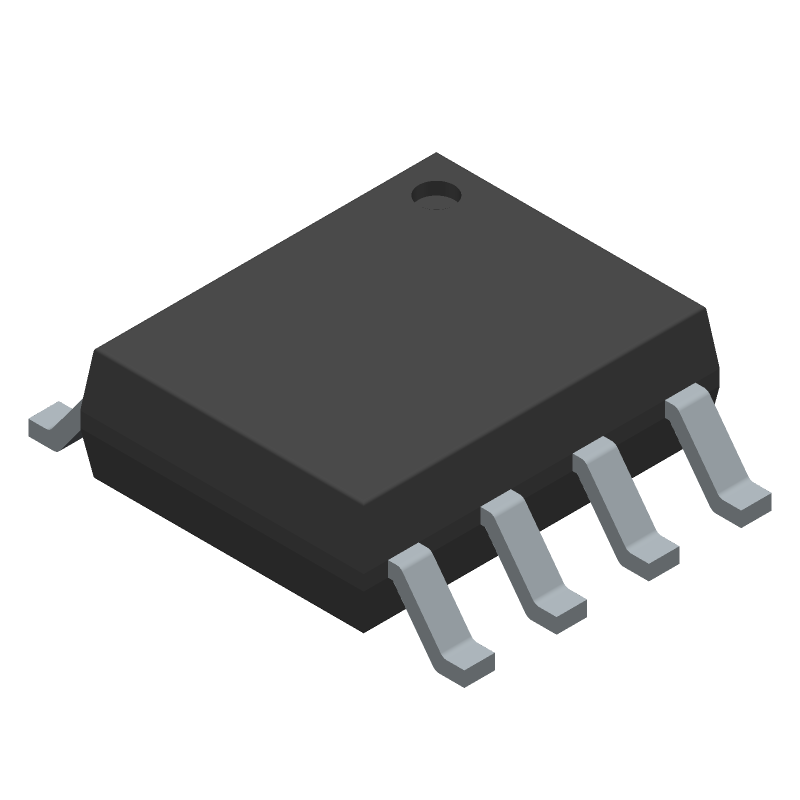
The NTMS4939NR2G is an N-CHANNEL JFET with a maximum operating temperature range of -55°C to 150°C. It has a continuous drain current of 8A and a drain to source breakdown voltage of 30V. The device has a drain to source resistance of 7mR and a maximum power dissipation of 800mW. It is packaged in a lead-free SOIC-8 package and is RoHS compliant.
Checking distributor stock and pricing after the page loads.
Onsemi NTMS4939NR2G technical specifications.
| Package/Case | SOIC |
| Continuous Drain Current (ID) | 8A |
| Drain to Source Breakdown Voltage | 30V |
| Drain to Source Resistance | 7mR |
| Drain to Source Voltage (Vdss) | 30V |
| Element Configuration | Single |
| Fall Time | 21.5ns |
| Gate to Source Voltage (Vgs) | 20V |
| Height | 1.5mm |
| Input Capacitance | 2nF |
| Lead Free | Lead Free |
| Length | 5mm |
| Max Operating Temperature | 150°C |
| Min Operating Temperature | -55°C |
| Max Power Dissipation | 800mW |
| Packaging | Tape and Reel |
| Polarity | N-CHANNEL |
| Power Dissipation | 1.35W |
| Rds On Max | 8.4mR |
| RoHS Compliant | Yes |
| Turn-Off Delay Time | 36.7ns |
| Turn-On Delay Time | 10.6ns |
| Width | 4mm |
| RoHS | Compliant |
No datasheet is available for this part.