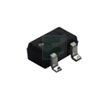
Single P-Channel Power MOSFET featuring a -30V Drain to Source Breakdown Voltage and a continuous Drain Current of 1.2A. This JFET offers a low Drain to Source Resistance of 165mR at a nominal Gate to Source Voltage of -1.15V. Designed for efficient switching, it exhibits a Turn-On Delay Time of 7.7ns and a Fall Time of 7.1ns. The component is housed in a compact SOT-323-3 package, measuring 2.2mm in length, 1.35mm in width, and 0.9mm in height, with a maximum power dissipation of 290mW. It operates within a temperature range of -55°C to 150°C and is RoHS compliant.
Checking distributor stock and pricing after the page loads.
Onsemi NTS4173PT1G technical specifications.
| Package/Case | SOT-323-3 |
| Continuous Drain Current (ID) | 1.2A |
| Drain to Source Breakdown Voltage | -30V |
| Drain to Source Resistance | 165mR |
| Drain to Source Voltage (Vdss) | -30V |
| Element Configuration | Single |
| Fall Time | 7.1ns |
| Gate to Source Voltage (Vgs) | 12V |
| Height | 0.9mm |
| Input Capacitance | 430pF |
| Lead Free | Lead Free |
| Length | 2.2mm |
| Max Operating Temperature | 150°C |
| Min Operating Temperature | -55°C |
| Max Power Dissipation | 290mW |
| Nominal Vgs | -1.15V |
| Package Quantity | 3000 |
| Packaging | Tape and Reel |
| Polarity | P-CHANNEL |
| Power Dissipation | 350mW |
| Radiation Hardening | No |
| Rds On Max | 150mR |
| Reach SVHC Compliant | No |
| RoHS Compliant | Yes |
| Threshold Voltage | -1.15V |
| Turn-Off Delay Time | 19.9ns |
| Turn-On Delay Time | 7.7ns |
| Width | 1.35mm |
| RoHS | Compliant |
No datasheet is available for this part.