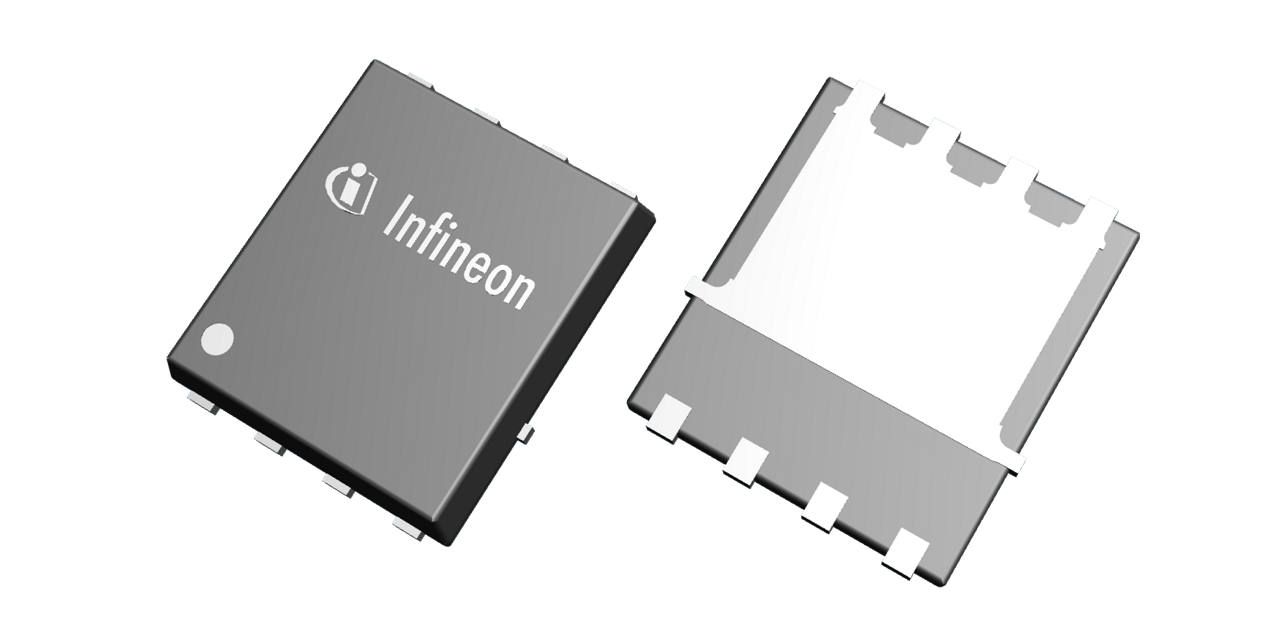
This device is an N-channel power MOSFET rated for 150 V drain-source voltage and up to 87 A drain current. It is specified with a maximum on-resistance of 9.3 mΩ and is housed in a SuperSO8 5x6 package identified by Infineon as PG-TDSON-8-7. The part belongs to the OptiMOS™ 5 150 V family and is intended for low-voltage drives, telecom equipment, and solar applications. Infineon highlights lower output charge, ultra-low reverse recovery charge, and increased commutation ruggedness for higher switching-frequency operation.
Checking distributor stock and pricing after the page loads.
Sign in to ask questions about the Infineon BSC093N15NS5 datasheet using AI. Get instant answers about specifications, features, and technical details, ideal for finding information in larger documents.
Sign In to ChatWidest selection of semiconductors and electronic components in stock and ready to ship ™
| Number of Terminals | 5 |
| Terminal Position | DUAL |
| Number of Elements | 1 |
| RoHS | Yes |
| Eccn Code | EAR99 |
| REACH | Compliant |
| Military Spec | False |
Download the complete datasheet for Infineon BSC093N15NS5 to view detailed technical specifications.
The embedded preview will load automatically when this section scrolls into view.
These are design resources that include the Infineon BSC093N15NS5
Design guide for a 3 kW dual-phase LLC converter using CoolMOS C7 MOSFETs and XMC4400 digital control for high-efficiency telecom and industrial SMPS applications.
Evaluation board featuring the 1EDN7550B gate driver with truly differential inputs (TDI) for bidirectional buck-boost conversion in low-voltage applications up to 84V.